

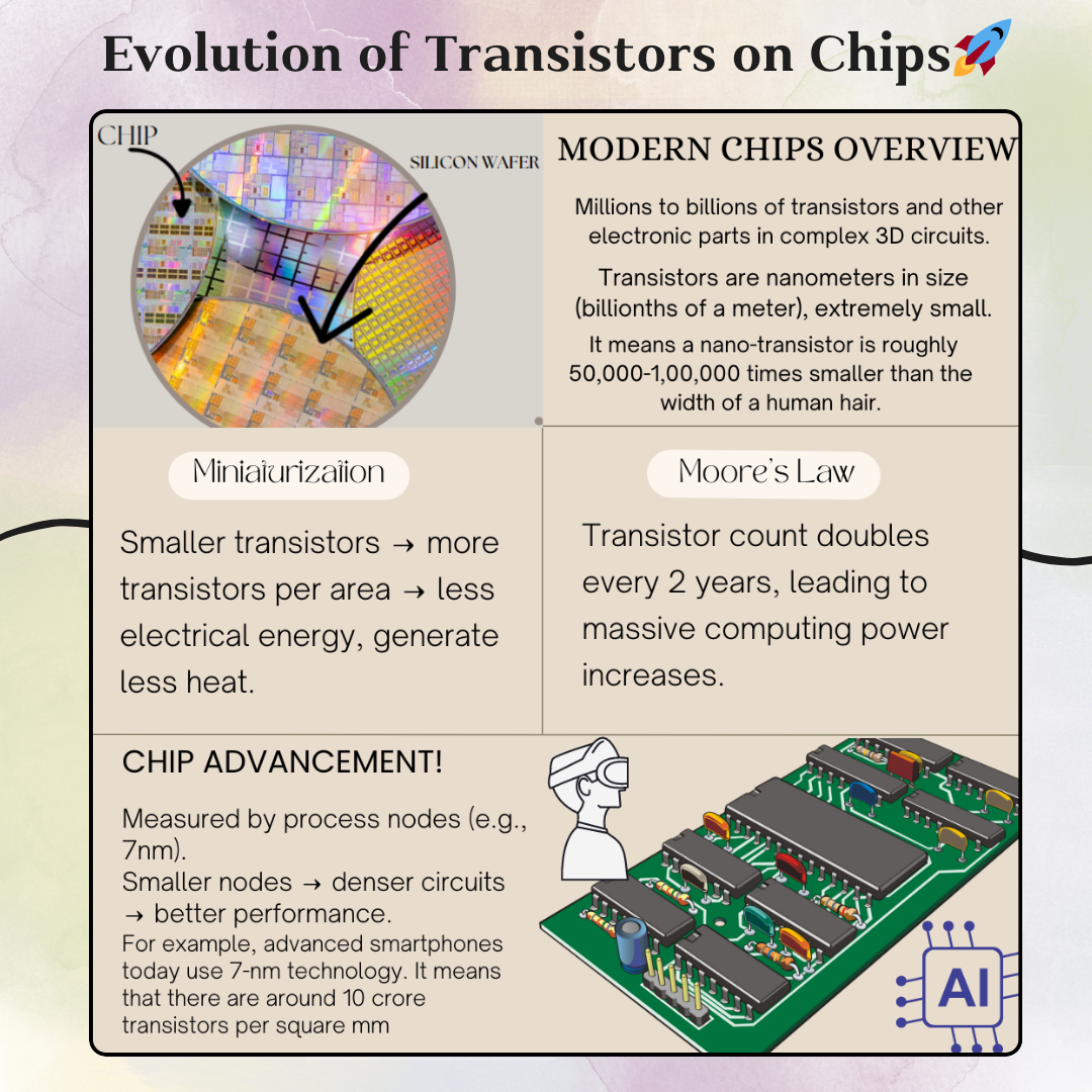
For six decades, Moore’s Law—the observation that the number of transistors on a microchip doubles every two years—has been the North Star of technological progress. Coined by Intel co-founder Gordon Moore in 1965, it fueled the digital revolution, enabling everything from smartphones to artificial intelligence. But as we approach the physical limits of silicon, a critical question looms: Is Moore’s Law dead, or is it evolving? At MIT, where engineers and physicists are reimagining computing’s future, the answer is clear: the spirit of Moore’s Law lives on, but its execution is undergoing a radical transformation.
The Golden Era: How Moore’s Law Built the Digital World
Moore’s Law was never a law of physics, but rather a self-fulfilling prophecy driven by ingenuity and economics. By shrinking transistors, the industry delivered exponential gains in speed, efficiency, and cost:
- 1960s–2000s: Transistors scaled from microns to nanometers. A modern chip holds over 50 billion transistors, each smaller than a virus.
- Economic Impact: Computing power became 1 trillion times cheaper since the 1950s, democratizing access to technology.
- Cultural Shift: It enabled the rise of the internet, genomics, and AI, reshaping society.
“Moore’s Law wasn’t just about transistors—it was a pact between science and capitalism,” says Dr. Lisa Su, MIT alumna and CEO of AMD. “Every industry rode this curve.”
The Cracks in the Foundation: Why Silicon Is Hitting a Wall
Is Moore’s Law finally hitting a wall, or are we just facing a temporary detour on the road to ever-faster computing?
The simple answer is: it’s complicated.
The fundamental challenge is physics. As transistors shrink to the size of atoms, quantum effects become increasingly dominant. Electrons don’t always behave nicely when confined to such tiny spaces. They can tunnel through barriers, creating unwanted current leakage and heat. Imagine trying to control a crowd of toddlers – the smaller the playpen, the harder it gets.
For years, engineers have ingeniously sidestepped these roadblocks. New materials, clever circuit designs, and innovative manufacturing processes have kept Moore’s Law alive, albeit with a slowing pace in recent years. The doubling of transistors now takes closer to two and a half years, a subtle but significant shift.
But the challenges are mounting. Traditional silicon-based transistors are approaching their fundamental limits. We’re bumping up against the atomic scale, where the very notion of a “transistor” as we know it starts to break down. Simply making things smaller isn’t enough anymore.
So, is this the end of the line? Not necessarily. History is littered with predictions of technological limits that were ultimately overcome. While the era of easy scaling may be over, innovation is far from dead.
Today, the traditional path of transistor scaling faces existential challenges:
- Physics Limits: At 3-nanometer scales, quantum effects like electron tunneling disrupt reliability.
- Economic Barriers: Building a single fabrication plant now costs $20 billion, limiting innovation to a few global players.
- Energy Costs: Data centers consume 2% of global electricity; doubling transistors no longer guarantees efficiency gains.
“We’re in the era of diminishing returns,” admits Dr. Jesús del Alamo, an MIT professor of electrical engineering. “But scarcity breeds creativity.”
Redefining Moore’s Law: MIT’s Blueprint for the Future
At MIT.nano and beyond, researchers are pioneering post-silicon paradigms to extend computing’s exponential trajectory:
1. Vertical Innovation: Chips That Think in 3D
- Stacked Transistors: Companies like Intel now build “3D” chips, layering components vertically.
- Quantum Integration: MIT’s Lincoln Lab is embedding photonic circuits with traditional silicon to accelerate data transfer.
2. Materials Revolution: Beyond Silicon
- Graphene & Carbon Nanotubes: MIT’s Tomás Palacios is developing ultra-efficient transistors from 2D materials.
- Gallium Nitride (GaN): Critical for next-gen power electronics, enabling faster charging and renewable energy grids.
3. Neuromorphic & Quantum Computing
- Brain-Inspired Chips: MIT’s “Brain-on-a-Chip” mimics neural networks, offering 1,000x efficiency gains for AI tasks.
- Quantum Leap: Startups like QuEra (spun out of MIT) are commercializing error-corrected quantum processors.
4. Software-Defined Hardware
- AI-Driven Design: MIT’s “AI Photonic Designer” algorithm creates optimized optical chips in hours, not years.
- RISC-V Architecture: Open-source chip designs, championed by MIT researchers, democratize hardware innovation.
Societal Implications: Who Controls the Future of Compute?
The end of classical Moore’s Law raises urgent questions:
- Geopolitics: With Taiwan producing 92% of advanced chips, the U.S. CHIPS Act aims to reshore manufacturing.
- Sustainability: Can we balance computing demands with net-zero goals? MIT’s Climate Grand Challenges initiative targets energy-efficient architectures.
- Equity: Will open-source hardware and AI democratize access, or will compute power remain concentrated?
“This isn’t just a technical problem—it’s a human one,” argues Dr. Vivienne Sze, MIT expert in energy-efficient AI. “We need systems that serve society, not just shareholders.”
Conclusion: The Law of Accelerating Returns
Moore’s Law is not dead—it’s metamorphosing. The next 60 years will prioritize heterogeneous integration (mixing silicon with quantum, photonic, and biological systems) over pure transistor density. At MIT, this philosophy is already embodied in projects like the MIT-IBM Watson AI Lab and the new $2 billion College of Computing.
“The future isn’t about smaller transistors,” says Dr. Anantha Chandrakasan, Dean of MIT Engineering. “It’s about smarter systems—where hardware, software, and societal needs co-evolve.”
As we stand at this inflection point, one truth endures: the human drive to innovate will always find a way. Moore’s Law was never the ceiling—it was the launchpad.